
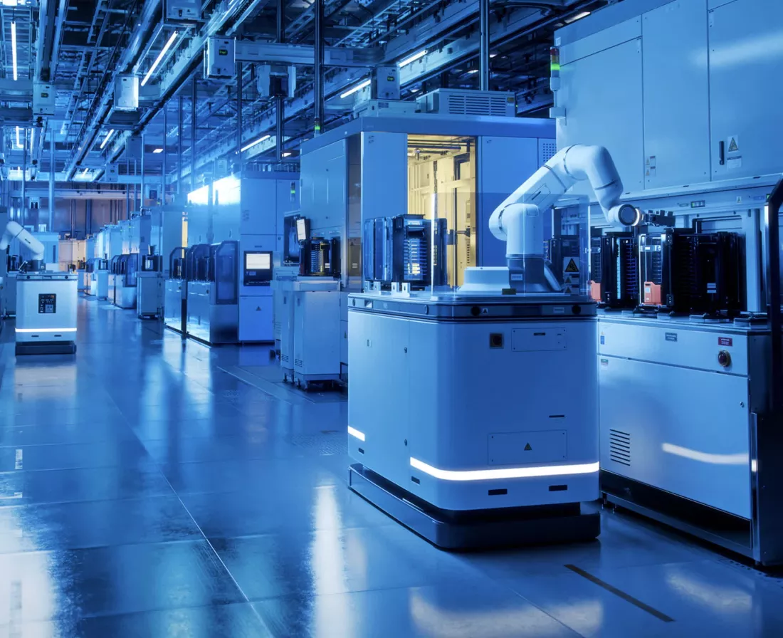
What simply occurred? TSMC has challenged Intel’s claims that it’s going to overtake the Taiwanese firm relating to making the world’s quickest computing chips by unveiling its A16 (1.6nm) manufacturing course of. TSMC says the huge demand from unnamed AI prospects meant the A16 expertise has been developed sooner than anticipated.
A16, set to enter manufacturing within the second half of 2026, will use main nanosheet transistors and what TSMC calls an “progressive” bottom energy rail resolution to deliver “revolutionary efficiency” to the wafer stage. Whereas conventional chip designs contain energy flowing from the highest down, the bottom energy rail system delivers energy from the underside. The corporate writes that it will assist tackle future AI necessities for hyperscale datacenters.
Intel says it additionally plans to combine bottom energy rail expertise into its 20A (2nm) and 18A (1.8nm) processes as early as 2025.
Based on TSMC’s roadmap, its 2nm N2 course of node is on monitor for manufacturing within the second half of 2025, the successor to its 3nm N3E expertise that’s now in manufacturing. A16 will comply with in 2026, combining TSMC’s Tremendous Energy Rail structure with its nanosheet transistors. It improves logic density by dedicating front-side routing assets to indicators, which ought to make it very best for HPC merchandise. In comparison with N2P, A16 will present an 8-10% pace enchancment, 15-20% energy discount, and as much as 1.10x chip density enchancment.
Kevin Zhang, TSMC’s senior vice chairman of enterprise improvement, stated the corporate does not consider it might want to use ASML’s new Excessive NA EUV lithography software machines for the A16 course of.
Intel stated final week that it will likely be the primary to make use of ASML’s machines, which price $373 million every, to assist develop its 14A (1.4nm) chips. Group Blue stated in February that 14A would assist it overtake TSMC in making the world’s quickest chips. Samsung, in the meantime, is aiming to mass produce its 1.4nm chips by 2027.
Intel’s foundry enterprise misplaced $7 billion final yr, one thing CEO Pat Gelsinger put all the way down to previous errors, together with the choice to not use ASML’s EUV machines. Intel later went again on its resolution and invested within the EUV machines, which ought to assist the foundry enterprise’ objective to interrupt even in about three years.
TSMC emphasised the advantages the A16 course of will deliver to AI chip makers. Zhang stated these corporations “actually need to optimize their designs to get each ounce of efficiency we’ve.” Earlier this yr, TSMC founder Morris Chang predicted that as much as 10 new fabs could be required for AI chip manufacturing.

