Questions:
1. Cubic boron arsenide is an ____________ semiconductor, meaning it can efficiently transport both electrons and holes. Fill in the blank.
2. Graphene lacks a critical property called a natural _______. This lacuna poses a significant challenge to its use as a traditional semiconductor despite its excellent electrical conductivity, high thermal conductivity, flexibility, and mechanical strength. Fill in the blank.
3. Re6Se8Cl2 is a recently discovered ___________ quantum material that allows particles called excitons to travel with minimal scattering and at 100- to 1,000-times faster than the speed of electrons in silicon, even at room temperature. This is a result of its crystal structure, which makes the material a potential candidate for robust semiconductors. Fill in the blank.
4. In this technique, thin films of semiconductor material are deposited on a surface by having its elemental constituents vaporise in a vacuum. It allows engineers to precisely control the thickness and composition of each layer of the semiconductor. Name this technique, commonly used to fabricate advanced electronic and optoelectronic devices.
5. In the early 1940s, researchers at Bell Labs introduced impurities in silicon and germanium to alter and study their electrical properties. These experiments led to the invention of X in 1947, boosting semiconductor technology and eventually winning its inventors a Nobel Prize in 1956. Name X.
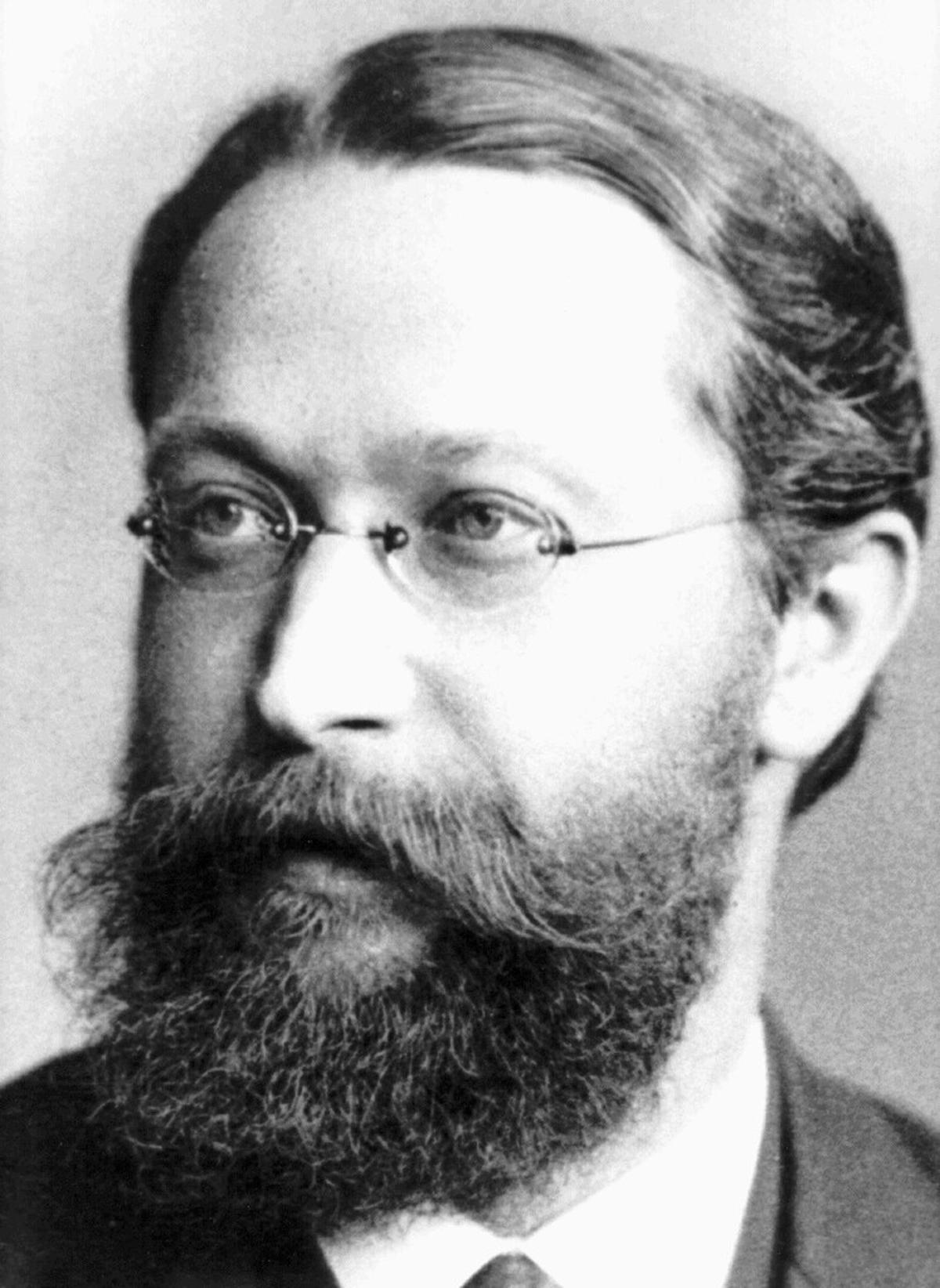
Visual:

Name this German physicist who, in 1874, discovered that in galena, a primary ore of lead, electric current flowed freely in only one direction. His discovery found practical application in the first crystal radio sets in the 1900s.
Answers:
1. Ambipolar
2. Bandgap
3. Superatomic
4. Molecular beam epitaxy
5. Transistor
Visual: Karl Ferdinand Braun
Published – September 27, 2024 11:30 am IST


